From semiconductor lead frames to vacuum devices, from sputtering targets to precision custom components —
KINMACHI delivers stable, reliable conductive and thermal substrate materials for high-end manufacturing, backed by 4N-grade purity and full-form supply capability.
I. Product Introduction
Product Name: Oxygen Free Copper C10100 (OFE). C10100 offers excellent corrosion resistance along with outstanding thermal and electrical properties, making it a key foundational material for high-end applications in electronics, semiconductors, vacuum technology, and precision instruments.
Core Positioning: Backed by more than 20 years of process expertise and investment in advanced production equipment, we manufacture ultra-high-purity oxygen-free copper C10100 to meet the demands of the rapidly evolving electronics industry.
Process Advantages: Our pioneering oxygen-free melting process strictly controls oxygen content below 3 ppm to eliminate porosity, while keeping hydrogen content below 1 ppm to ensure material purity and reduce oxide formation. Combined with 10–50 zone-refining purification passes for ultimate impurity removal and PPB-level precision testing capability, we guarantee reliable delivery of high-conductivity oxygen-free copper.
II. Core Technical Specifications
KINMACHI enforces strict full-process control over the key physical and chemical parameters of C10100, ensuring every batch meets the stringent requirements of high-end electronics and semiconductor applications:
| Item | Specification / Description | Remarks |
| Grade | Oxygen Free Copper C10100 (OFE) | Internationally recognized high-purity oxygen-free copper grade |
| Copper Content (Cu+Ag) | ≥ 99.99% (4N grade) | Extremely high purity, minimal impurities |
| Oxygen Content | < 3 ppm | Oxygen-free melting technology prevents hydrogen embrittlement |
| Conductivity | ≥ 102.5% IACS | Excellent electrical performance |
| Impurity Control | P, Bi, Sb, As, Fe, Pb, Ni, Sn, S, Zn all ≤ 0.0003% | Precise trace-element control |
| Grain Size | Uniform, fine grain; customizable | Meets diverse processing and forming requirements |
III. Chemical composition
| Item | Cu | Ag | As | Bi | Cd | Fe | Mn | Ni | O | P | Pb | S | Sb | Se | Sn | Te | Zn |
| Min | 99.99 | ||||||||||||||||
| Max | – | 0.0025 | 0.0005 | 0.0002 | 0.0001 | 0.001 | 0.0005 | 0.001 | 3ppm | 0.0003 | 0.0005 | 0.0015 | 0.0004 | 0.0002 | 0.0002 | 0.0002 | 0.0001 |
IV. Product Forms & Applications
KINMACHI offers a full range of C10100 oxygen-free copper solutions, spanning the complete product spectrum from raw materials to finished parts, to meet diverse industrial application needs:
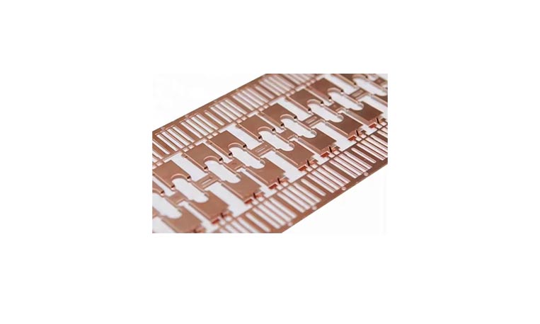
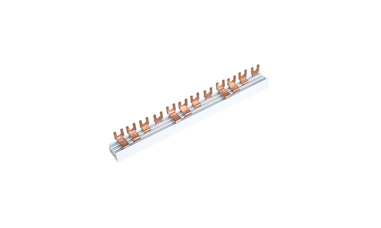
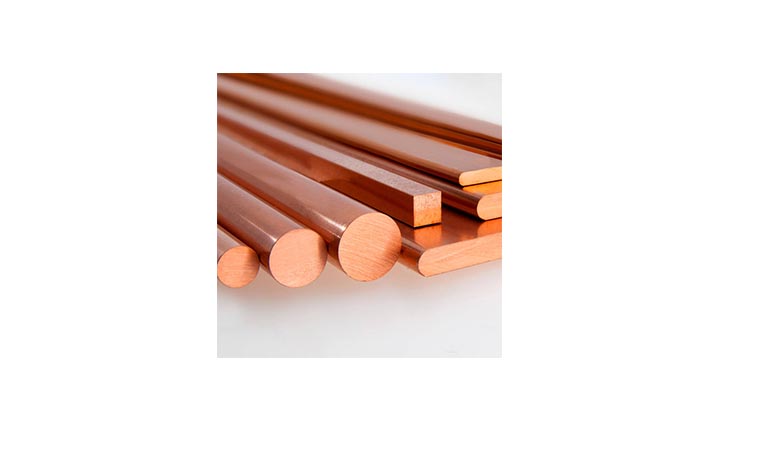
| Sheet & Strip Suitable for semiconductor lead frames, electronic component heat sinks, and glass-to-metal seals — applications with stringent requirements for conductivity, thermal performance, and dimensional precision. | Tube, Rod & Wire Suitable for vacuum device structural parts, high-conductivity cables, and precision instrument components, combining high purity with excellent machinability. |
| Sputtering Target Suitable for semiconductor sputtering processes, optical coatings, cavity resonators, and superconductor substrates, meeting high-end coating purity requirements. | Custom Forms Copper granules, chip heat-dissipation heat pipes, and other custom-shaped parts, flexibly formed to customer structural and process requirements. |
V. Why KINMACHI
| 20+ Years of Process Expertise Sustained investment in advanced production equipment and process R&D, with deep insight into the evolving material needs of the electronics industry. |
| Pioneering Oxygen-Free Melting Process Oxygen content strictly controlled below 3 ppm and hydrogen below 1 ppm, eliminating porosity and hydrogen-embrittlement risk at the source — industry-leading material purity. |
| 10–50 Zone-Refining Purification Passes An ultimate impurity-removal process combined with PPB-level precision testing capability ensures stable delivery of high conductivity and other key performance metrics. |
| One-Stop Full-Form Supply Sheet & strip, tube/rod/wire, sputtering targets, and custom-shaped parts — one supplier covers every form across the value chain, reducing multi-vendor coordination costs. |
| Rapid Response & Customization Supports small-batch sampling and custom shaping, adapting to the fast-iteration needs of new product development. |
Technical Consultation & Selection Support
If you are evaluating material solutions for lead frames, vacuum device structural components, sputtering targets, or other high-conductivity/thermal applications, please contact the KINMACHI technical team. We offer grade selection guidance, sample production, and bulk supply support.